Search Other Blog

Showing posts with label Voltage Regulators. Show all posts

NE555 Voltage doubler circuit

NE555 Voltage doubler circuitThe circuit diagram of a absolute simple voltage doubler application NE555 timer is apparent here. Actuality IC NE555 is active as an astable mutivibrator operating at about 9KHz. The abject of the two transistors (Q1 and Q2) is shorted and achievement of the astable multivibrator (pin 3) is affiliated to it.

When the achievement of astable multivibrator is low, Q1 will be OFF and Q2 will be ON. The abrogating terminal of the capacitor C3 will be shorted to arena through T2 and it will be answerable to the ascribe accumulation voltage. When the achievement of the astable multi vibrator is high, transistor Q1 will be ON and transistor Q2 will be OFF. The capacitor C4 will be answerable to the voltage beyond capacitor C3 additional the ascribe accumulation voltage. This is how the circuit works.

This voltage doubler circuit can bear alone up to 50mA achievement accepted and aloft that accepted absolute the achievement voltage will be badly reduced. The absolute achievement voltage will be about 19V for a 12V DC ascribe and aswell the achievement voltage will be a bit unstable. Anyway, for low accepted applications this circuit is able-bodied enough.
READ MORE - NE555 Voltage doubler circuit

LM1758 A Switching Regulator Circuit

LM1758 A Switching Regulator Circuit
The National Semiconductor LM 1578 A is very a switching regulator Which should easily be set up for such dc-to-dc voltage .conversion circuits as the buck, boost, and inverting configurations. The LM 1578 A features a distinctive comparator input stage Which not just} has separate pins for both the inverting and non-inverting inputs, but as well offers an internal 1.0 V reference to every input, thereby simplifying circuit design and PC board layout.

The output can switch upto 750 m A and has output pins for its collector and emitter to market design flexibility. An external current limit terminal tend to be referenced to either the ground or the Vin terminal, depending upon the application. In addition, the LM 1578 A has an on board oscillator, Which sets the switching frequency with other a single external capacitor in one < 1 Hz to 100 kHz (typical). It operates in one supply voltages of 2 V to 40 V. it's really provided with other current limit and thermal shutdown. Duty cycle up to 90 %. Functional diagram is given in figure.
READ MORE - LM1758 A Switching Regulator Circuit

Dual Power Supply using LM 320 and LM 340

Dual Power Supply using LM 320 and LM 340
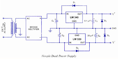
Number of signs needed and bipolar integrated circuits (double V ± o) supplies. This can be done easily with two three-terminal regulators, as illustrated in Fig. Faced with the CA phase is provided by the transformer secondary and a center tap to ground. The only full-wave bridge converts these into positive and negative voltages (with respect to the center tap to ground). Filtration (to ground) is provided by the capacitors C1 and C2.

The LM 340 provides positive voltage regulation, while the LM 320 regulates the negative voltage. It is very important to mention that LM 320 has a pin configuration different from the LM 340. The case of the 320 LM is not a field. So care must be taken while mounting the negative regulator.

Diodes provide protection, but make sure you are not invested. Diodes DI and D2 ensure that transients in the outputs of the controller output does not lead to a potential above its inputs and cause damage to the regulators. Furthermore, the two regulators are not activated simultaneously. If this occurs, the controller output can be driven slowly to the potential of the fastest. The diodes D3 and D4 prevent these reversed polarity at startup.
Dual Power Supply using LM 320 and LM 340
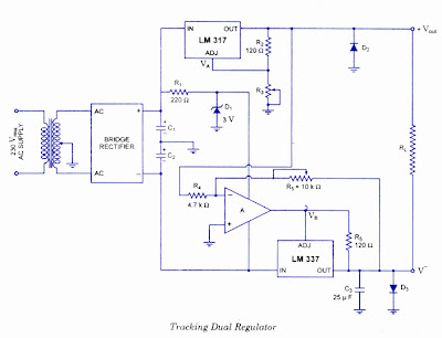
Many applications require many different sources of energy supply. One solution is the construction of several independent regulators. However, very often, it is important that all these voltages track. That is, if one of the voltages up 2%, it is best that all voltages are on the same amount. Can be achieved by adding an op amp voltage regulator for three-terminal adjustable.

The circuit of the figure provides a close current limiting and thermal for negative and positive output voltage. The positive voltage regulator produces an adjustable positive regulator LM 317 IC, as it was in the figure.

The positive sign is always regulated 1.2 V more positive than the voltage across R3 (on pin adjustment). This output voltage is used as the input of an inverting amplifier. The amplifier A is the input stage of this amplifier, and voltage regulator LM 337 negative is the power output stage. Consequently, the negative regulated output voltage V "is amplified and inverted version of the regulated positive voltage V +. Current limiting and thermal shutdown are independently provided by the LM 317 (for the positive output) and LM 337 (to output negative). The operational amplifier ensures that the negative output voltage tracks the positive output from the conduct of the LM 337 adjust pin to + 1.2 V above the negative output required. Given the LM 337 is within the negative feedback loop of operational amplifier, this offset + 1.2 V appears between the amplifier and the regulator, not the regulator output.
READ MORE - Dual Power Supply using LM 320 and LM 340

3A Switching Regulator using IC LM317

3A Switching Regulator using IC LM317When compared to linear voltage regulators the switching voltage regulators are power . case of linear voltage regulators the between the input and output voltage wasted and for switching regulators no such wastage and that’s why the switching regulators have power ranging up to . In words, the switching regulator operates by taking bits of energy from the input voltage and then transferring it to the output with of a solid state switch and circuitry. Since the switching is either open or closed at any moment, no energy is wasted across it. The circuit controls the duty cycle of the solid state switch in determines rate at energy is transferred to the output.

The electronic circuit given here is of and low switching regulator using the IC LM317 deliver up to 3A of current. The input voltage of this circuit is between to 35V DC output voltage adjusted between .8 to 32V DC. The output voltage adjusted by using the POT R4.

Notes.

  • Assemble the circuit on a good quality PCB.
  • C4 and C3 must be a solid tantalum capacitor.
  • Transistor T1 and IC1 require heat sinks.
  • L1 can be a 600uH inductor.
READ MORE - 3A Switching Regulator using IC LM317